


Combinational circuit과 sequential circuit이 섞인 회로를 구성할 때는 delay를 고려하여 클럭의 frequency를 정해야 합니다. 오늘은 Intel Quartus로 timing analysis하는 방법을 알아보겠습니다.
- IDE: Intel Quartus 18.1
- Device: Cyclone V 5CSXFC6D6F31C6(밑에서 6번째)
- Simulation: ModelSim-Altera, Verilog HDL
- Project Name & the name of Top-level: cla32_clk
목차
1. 예제 코드
1.1. cla32.v
1.2. reg32.v
1.3. _dff_r.v
1.4. cla32_clk.v
2. Timing Analysis
3. 글 마무리
4. 참고 자료
1. 예제 코드
32-bit Carry Look-Ahead(CLA) Adder with clock을 만들겠습니다.
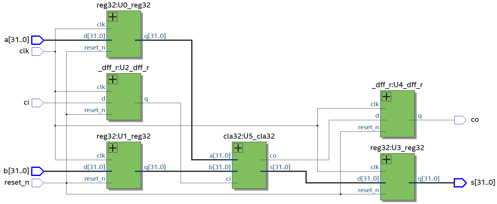
참고로 합성 후 RTL View는 위와 같이 나옵니다.
1.1. cla32.v
module cla32(a, b, ci, s, co);	//32-bit Carry Look-Ahead Adder
	input [31:0] a, b;	//operand
	input ci;				//carry in
	output [31:0] s;		//sum
	output co;				//carry out
	wire w0, w1, w2, w3, w4, w5, w6, w7;

	clb4 U0_clb4(a[3:0], b[3:0], ci, s[3:0], w0);
	clb4 U1_clb4(a[7:4], b[7:4], w0, s[7:4], w1);
	clb4 U2_clb4(a[11:8], b[11:8], w1, s[11:8], w2);
	clb4 U3_clb4(a[15:12], b[15:12], w2, s[15:12], w3);
	clb4 U4_clb4(a[19:16], b[19:16], w3, s[19:16], w4);
	clb4 U5_clb4(a[23:20], b[23:20], w4, s[23:20], w5);
	clb4 U6_clb4(a[27:24], b[27:24], w5, s[27:24], w6);
	clb4 U7_clb4(a[31:28], b[31:28], w6, s[31:28], co);
endmodule

module fa(a, b, ci, s, co);	//full adder
	input a, b;		//operand
	input ci;		//carry in
	output s;		//sum
	output co;		//carry out
	wire w0, w1, w2;

	assign s=a^b^ci;
	assign co=a&b|a&ci|b&ci;
endmodule

module rca4(a, b, ci, s, co);	//4-bit Ripple Carry Adder
	input [3:0] a, b;	//operand
	input ci;			//carry in
	output [3:0] s;	//sum
	output co;			//carry out
	wire w0, w1, w2;

	fa U0_fa(a[0], b[0], ci, s[0], w0);
	fa U1_fa(a[1], b[1], w0, s[1], w1);
	fa U2_fa(a[2], b[2], w1, s[2], w2);
	fa U3_fa(a[3], b[3], w2, s[3], co);
endmodule

module carry4(a, b, ci, co);	//4-bit Carry Look-Ahead Carry
	input [3:0] a, b;	//operand
	input ci;			//carry in
	output co;			//carry out
	wire [3:0] g, p;

	assign g=a&b;
	assign p=a|b;

	assign co=g[3]|p[3]&(g[2]|p[2]&(g[1]|p[1]&g[0]))|p[3]&p[2]&p[1]&p[0]&ci;
endmodule

module clb4(a, b, ci, s, co);	//4-bit Carry Look-Ahead Block
	input [3:0] a, b;
	input ci;
	output [3:0] s;
	output co;

	rca4 U0_rca4(a, b, ci, s,);
	carry4 U1_carry4(a, b, ci, co);
endmodule
CLA Adder에 대한 설명은 https://sooseongcom.com/post/adder-subtractor#2-carry-look-ahead-adder를 참고하시기 바랍니다.
1.2. reg32.v
module reg32(clk, reset_n, d, q);
	input clk, reset_n;
	input [31:0] d;
	output reg [31:0] q;

	always @ (posedge clk or negedge reset_n)
	begin
		if(reset_n==0)	q<=0;
		else	q<=d;
	end
endmodule
32-bit register입니다.
1.3. _dff_r.v
module _dff_r(clk, reset_n, d, q);
	input clk, reset_n, d;
	output reg q;

	always @ (posedge clk or negedge reset_n)
	begin
		if(reset_n==0)	q<=0;
		else	q<=d;
	end
endmodule
D Flip-flop입니다.
1.4. cla32_clk.v
module cla32_clk(clk, reset_n, a, b, ci, s, co);
	input clk, reset_n;
	input [31:0] a, b;	//operand
	input ci;				//carry in
	output [31:0] s;		//sum
	output co;				//carry out
	wire [31:0] w_a, w_b;	//outputs of registers
	wire w_ci;              //output of D Flip-flop
	wire [31:0] w_s;		//input of register
	wire w_co;              //input of D Flip-flop

	//input registers
	reg32 U0_reg32(clk, reset_n, a, w_a);
	reg32 U1_reg32(clk, reset_n, b, w_b);
	_dff_r U2_dff_r(clk, reset_n, ci, w_ci);

	//output registers
	reg32 U3_reg32(clk, reset_n, w_s, s);
	_dff_r U4_dff_r(clk, reset_n, w_co, co);

	//combinational circuit
	cla32 U5_cla32(w_a, w_b, w_ci, w_s, w_co);
endmodule
input인 a, b, ci와 output인 s, co를 모두 register 또는 D Flip-flop로 할 것입니다.
Clock의 이름은 clk로 했습니다.
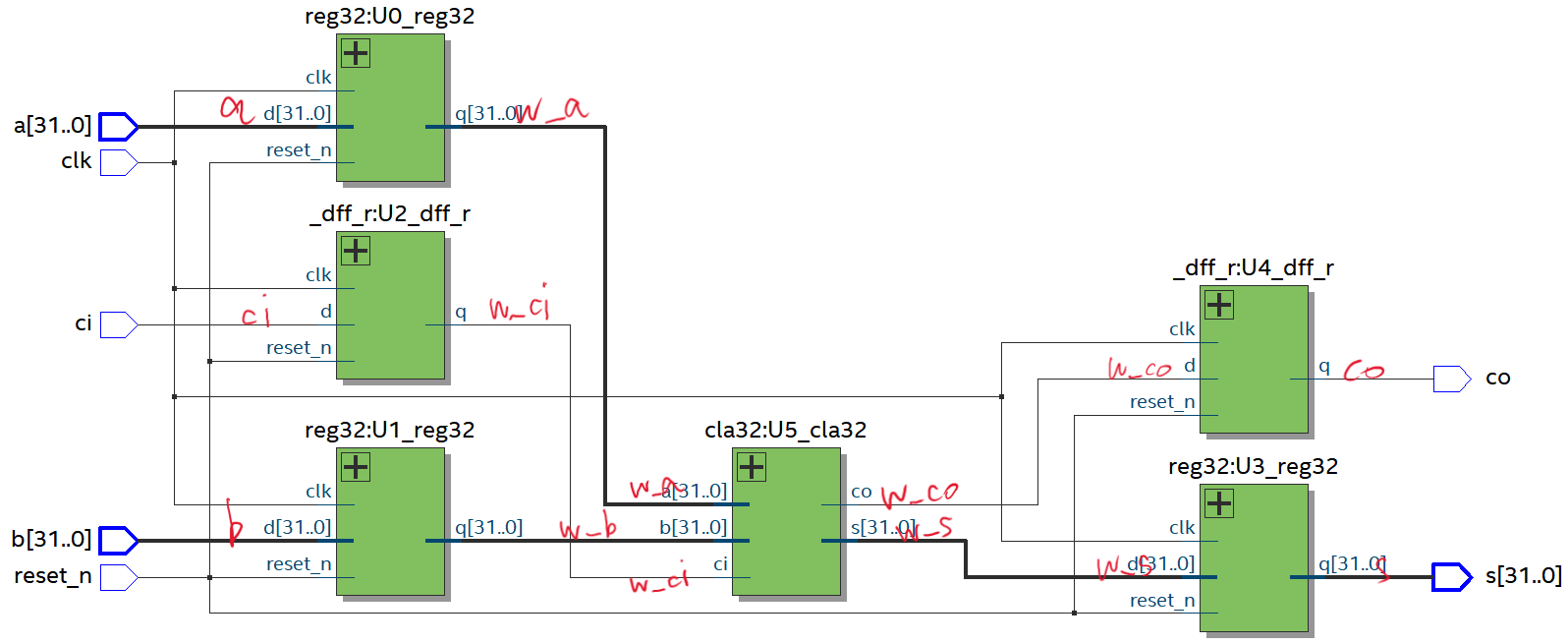
이해하기 쉽도록 빨간 글씨로 표시해 드렸으니 참고하세요.^^
2. Timing Analysis
2.1. Tools→Timing Analyzer로 들어갑니다.
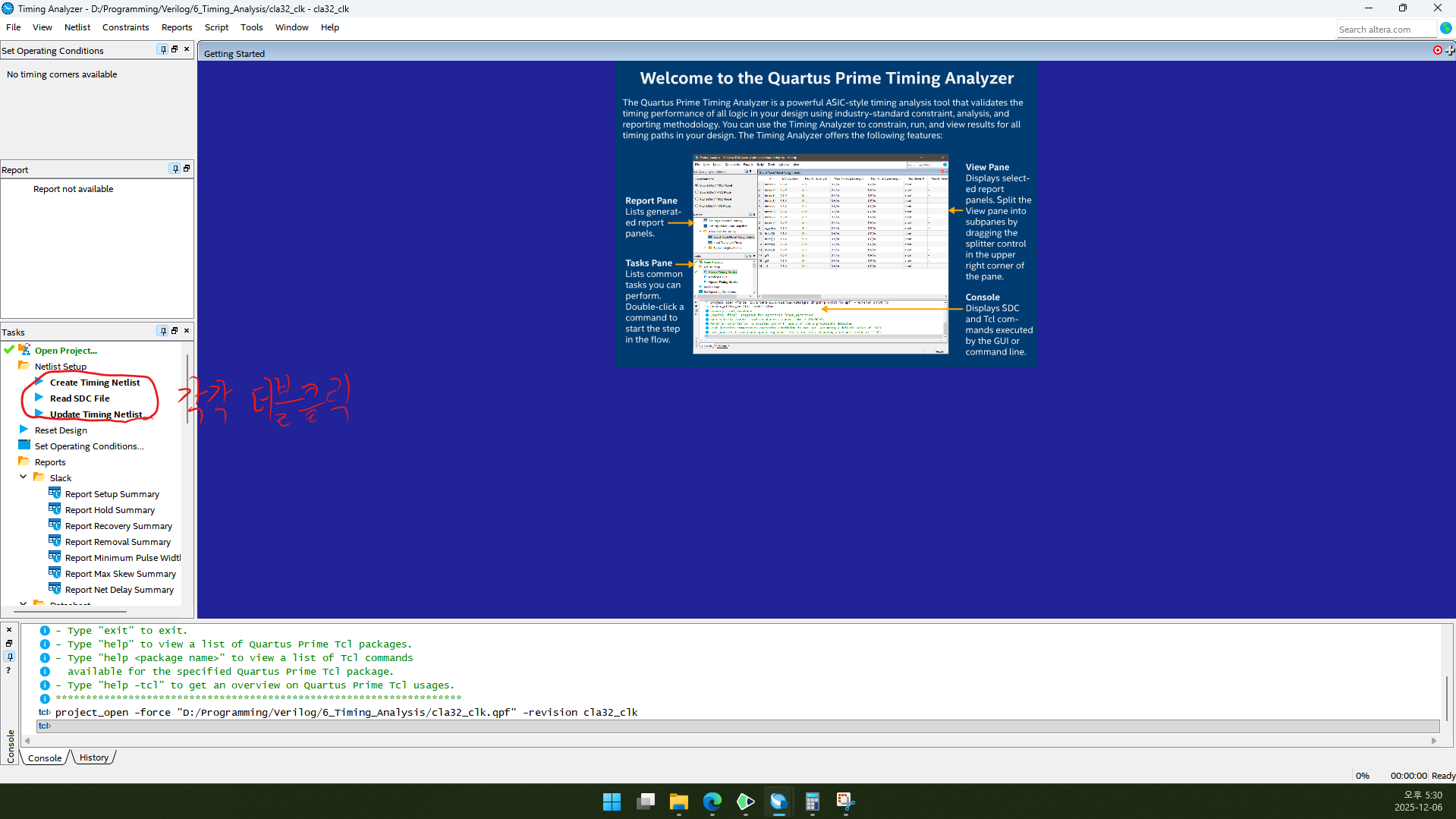
2.2. Create Timing Netlist, Read SDC File, Update Timing Netlist를 각각 더블클릭합니다.
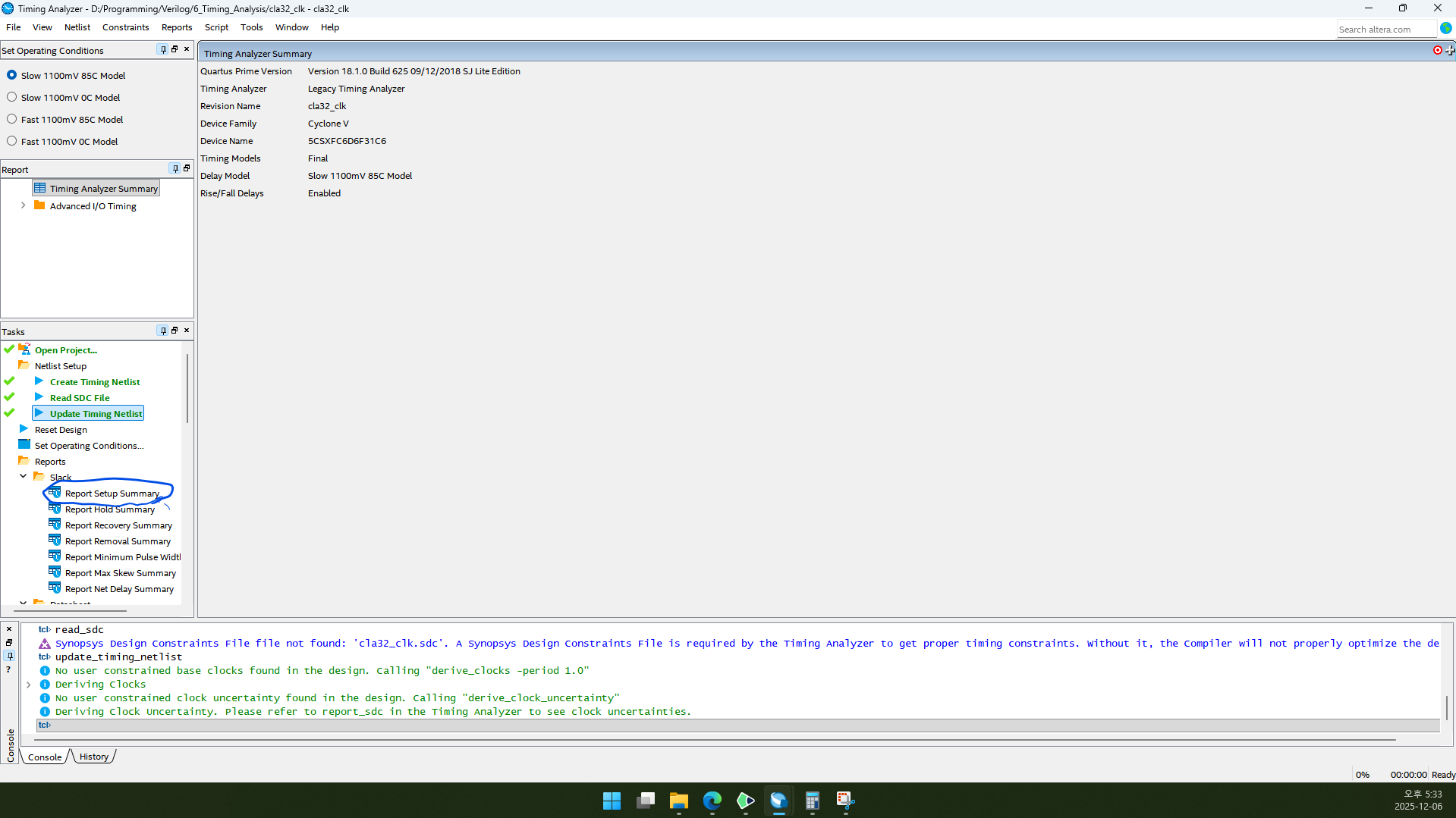
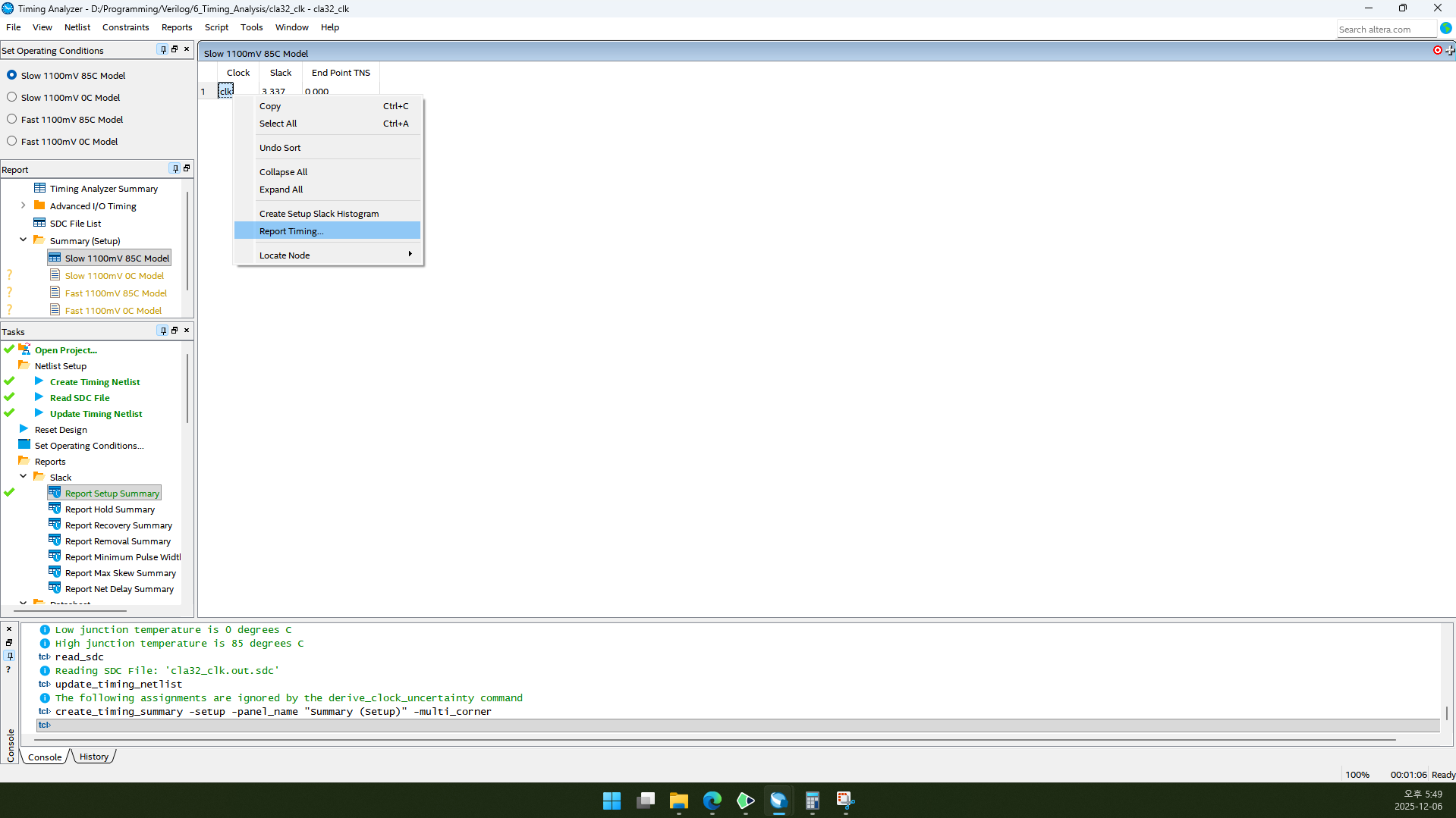
2.3. Report Setup Summary를 더블클릭합니다.
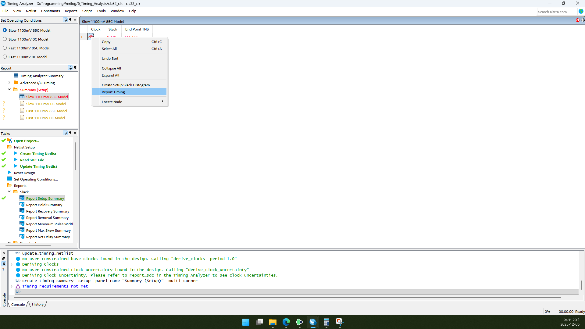
2.4. Top module에 있는 clock이 창의 Clock 항목에 나타납니다. 예제 코드대로 하면 clk가 있을 것입니다. clk를 오른쪽 클릭하고 Report Timing을 클릭합니다.
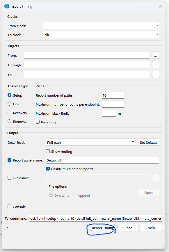
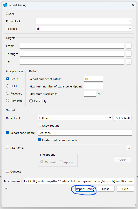
2.5. Report Timing을 클릭합니다.
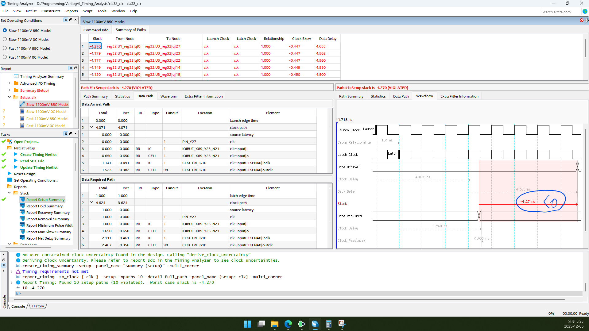
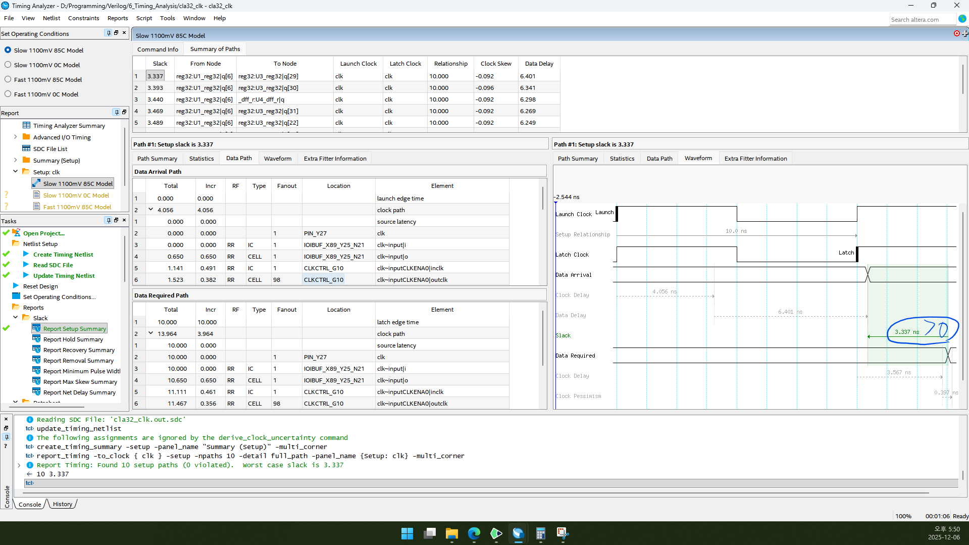
2.6. 오른쪽 아래를 보면 Slack이 -4.27 ns로 음수인 것을 볼 수 있습니다. 이는 clock 주기 안에 데이터가 전달되지 않았다는 뜻이므로 clock 주기를 늘려야 합니다.
참고) 초기 clock 주기는 1ns입니다.
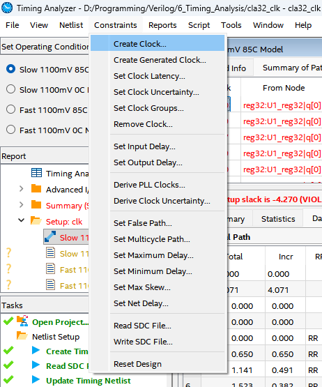
2.7. Constraints→Create Clock...을 클릭합니다.
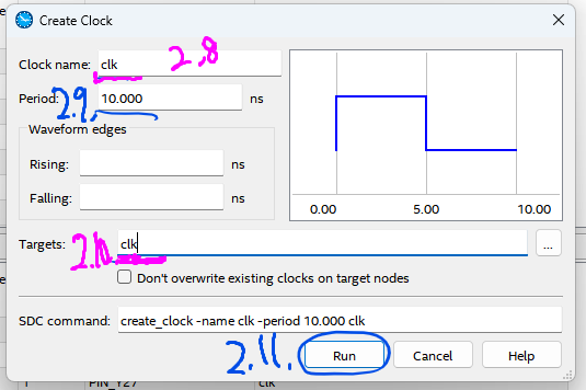
2.8. Clock name은 Top module에서 사용하는 clock의 이름(예제 기준: clk)을 입력합니다.
2.9. Period는 적당히 큰 숫자를 입력합니다. 저는 기본값인 10.000 그대로 두었습니다.
2.10. Targets는 Top module에서 사용하는 clock의 이름(예제 기준: clk)을 입력합니다.
2.11. Run을 클릭합니다.
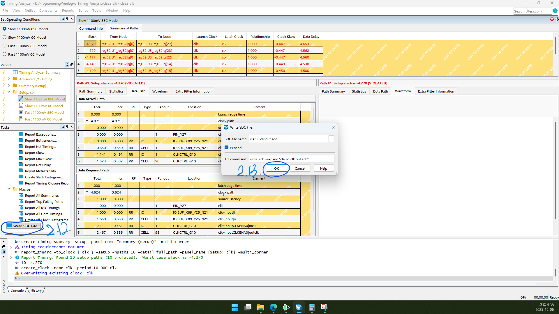
2.12. 왼쪽 Tasks를 아래로 스크롤하면 Write SDC File...이 있습니다. 더블클릭합니다.
2.13. SDC file name을 확인하고 OK를 클릭합니다.
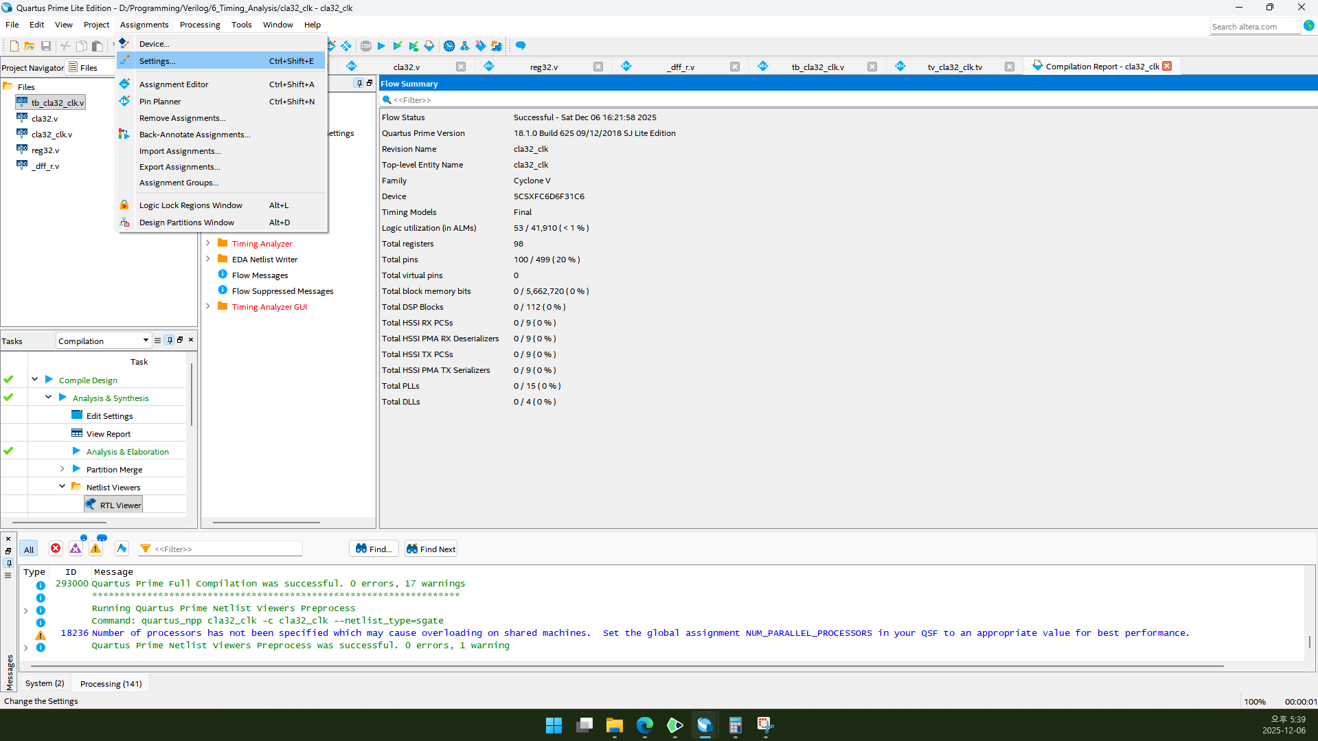
2.14. 다시 Quartus 메인 창으로 돌아와서 Assignments→Settings...로 들어갑니다.
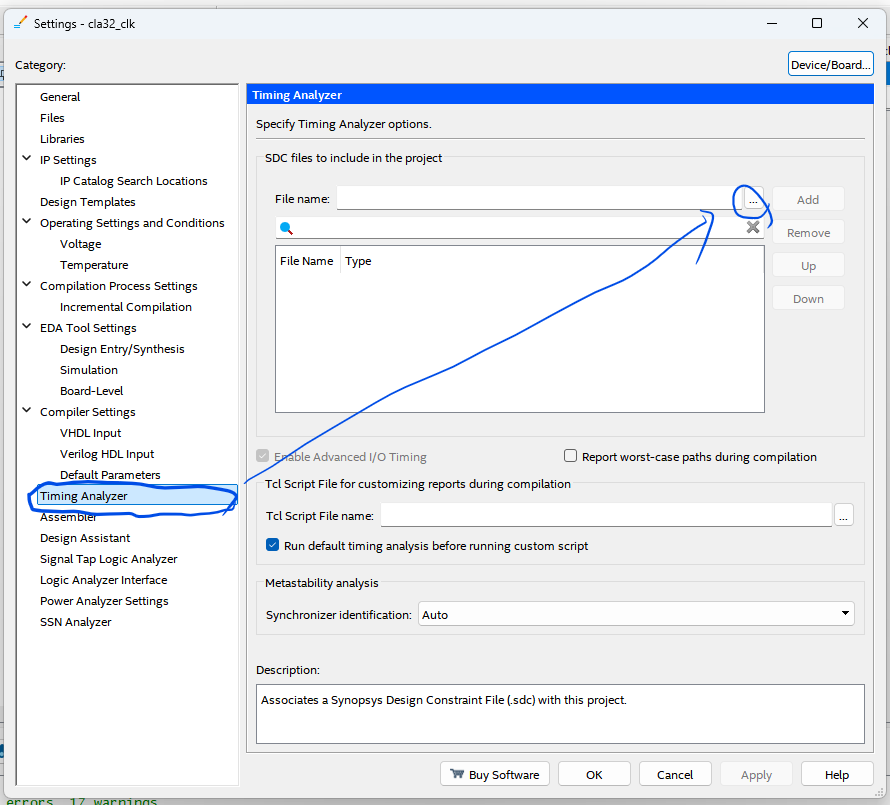
2.15. Timing Analyzer 카테고리로 들어가서 File name ...을 클릭합니다.
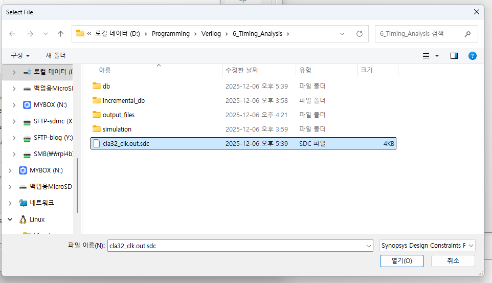
2.16. 방금 만든 SDC 파일을 선택합니다.(확장명이 .sdc인 것을 선택하세요.)
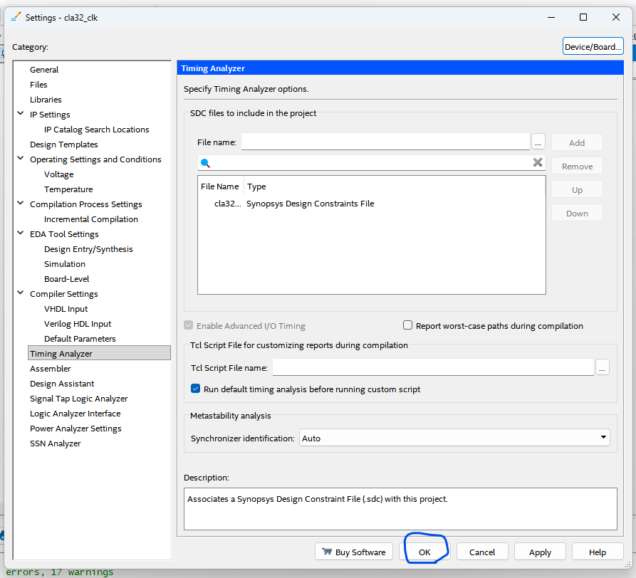
2.17. OK를 클릭합니다.
2.18. 다시 컴파일합니다.(Ctrl+L)
2.19. Timing Analyzer 창으로 다시 돌아갑니다.
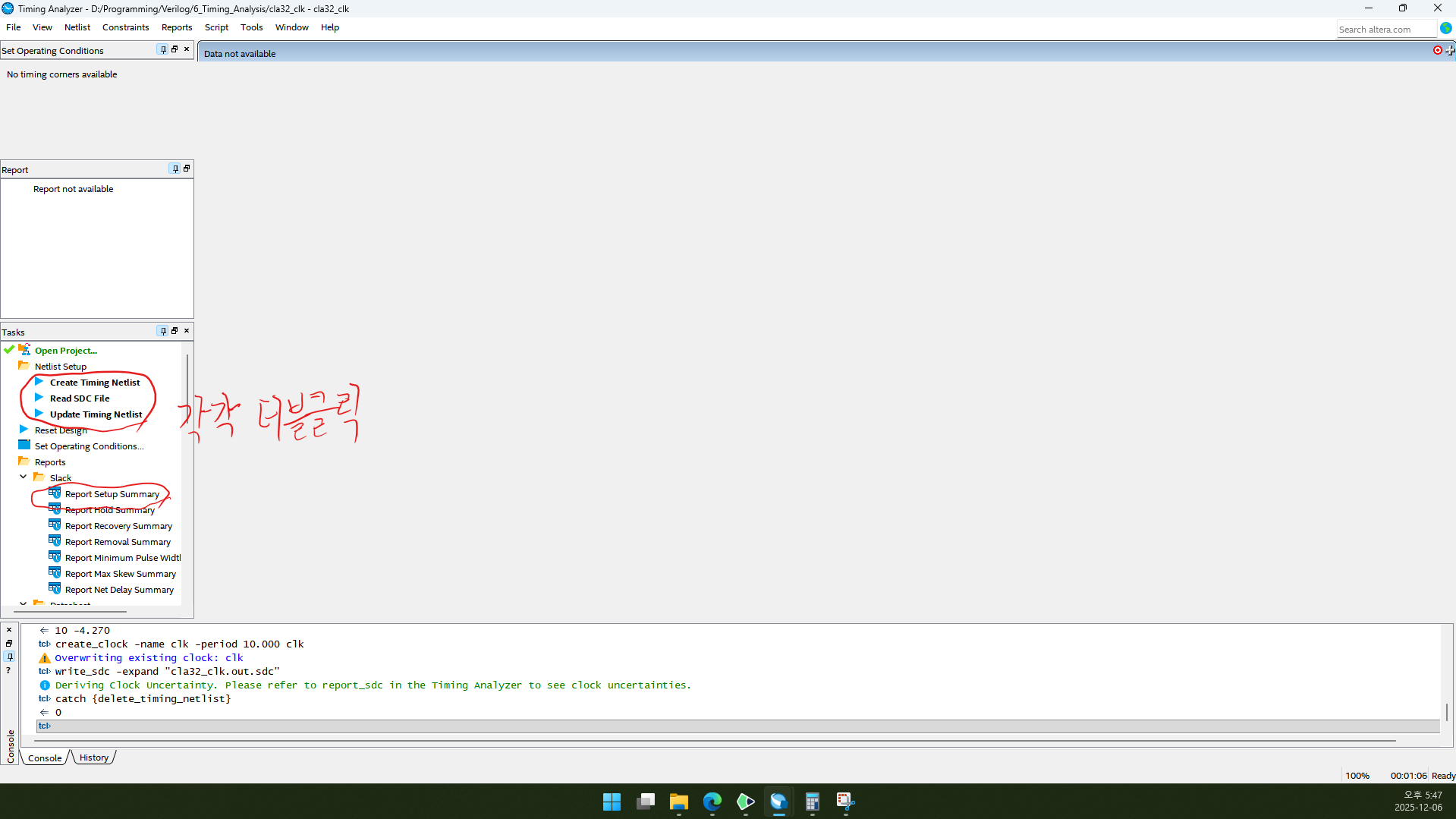
2.20. Create Timing Netlist, Read SDC File, Update Timing Netlist, Report Setup Summary를 각각 더블클릭합니다.
2.21. clk를 오른쪽 클릭하고 Report Timing을 클릭합니다.
2.22. OK를 클릭합니다.
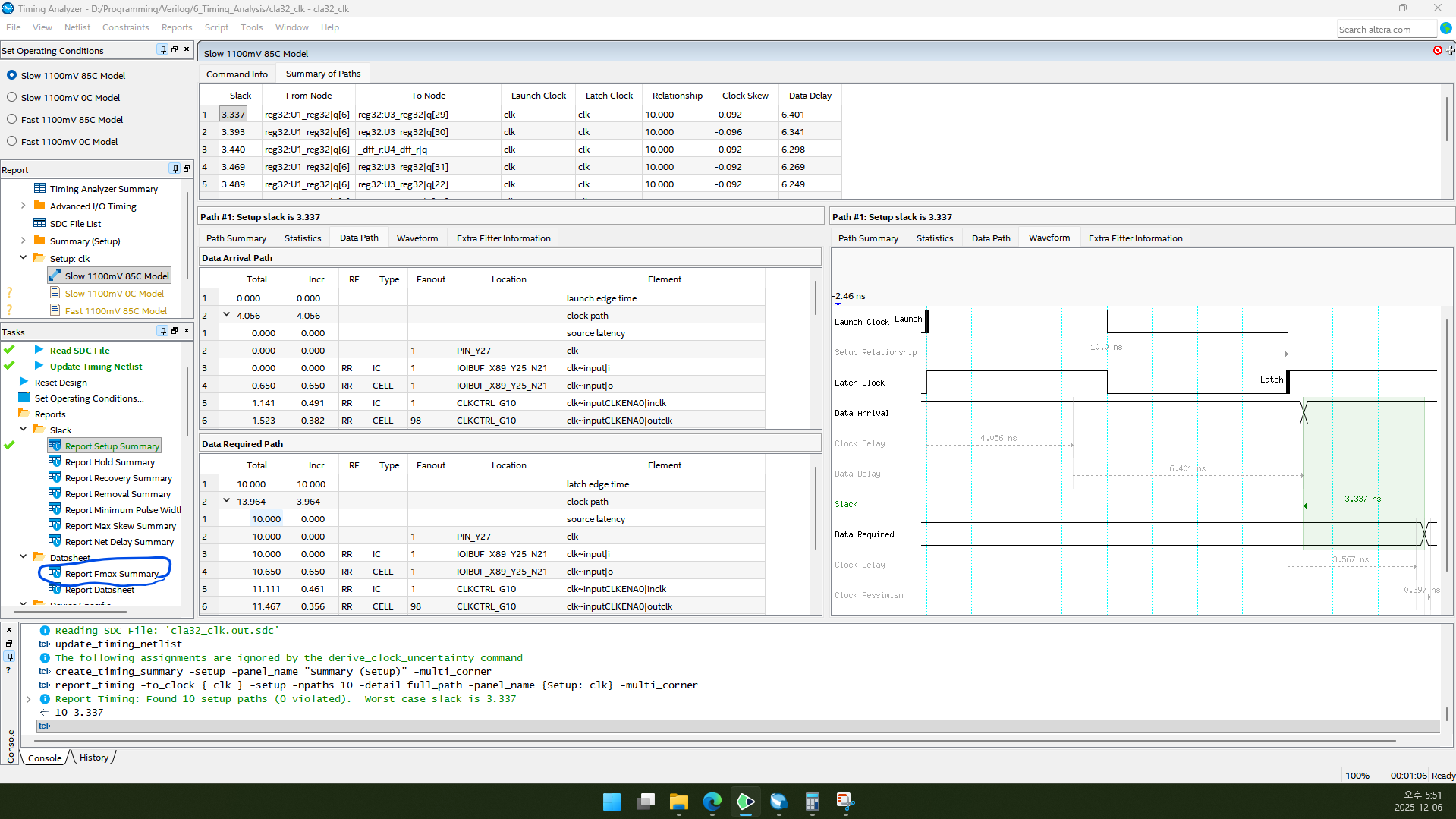
2.23. 오른쪽 아래를 보면 Slack이 3.337 ns로 양수인 것을 볼 수 있습니다. 그러면 성공입니다. 그렇다고 clock 주기를 10ns로 계속 사용할 수는 없으니 clock 주기의 최솟값을 찾아 봅시다.
2.24. 왼쪽 Tasks에서 Report Fmax Summary를 더블클릭합니다.
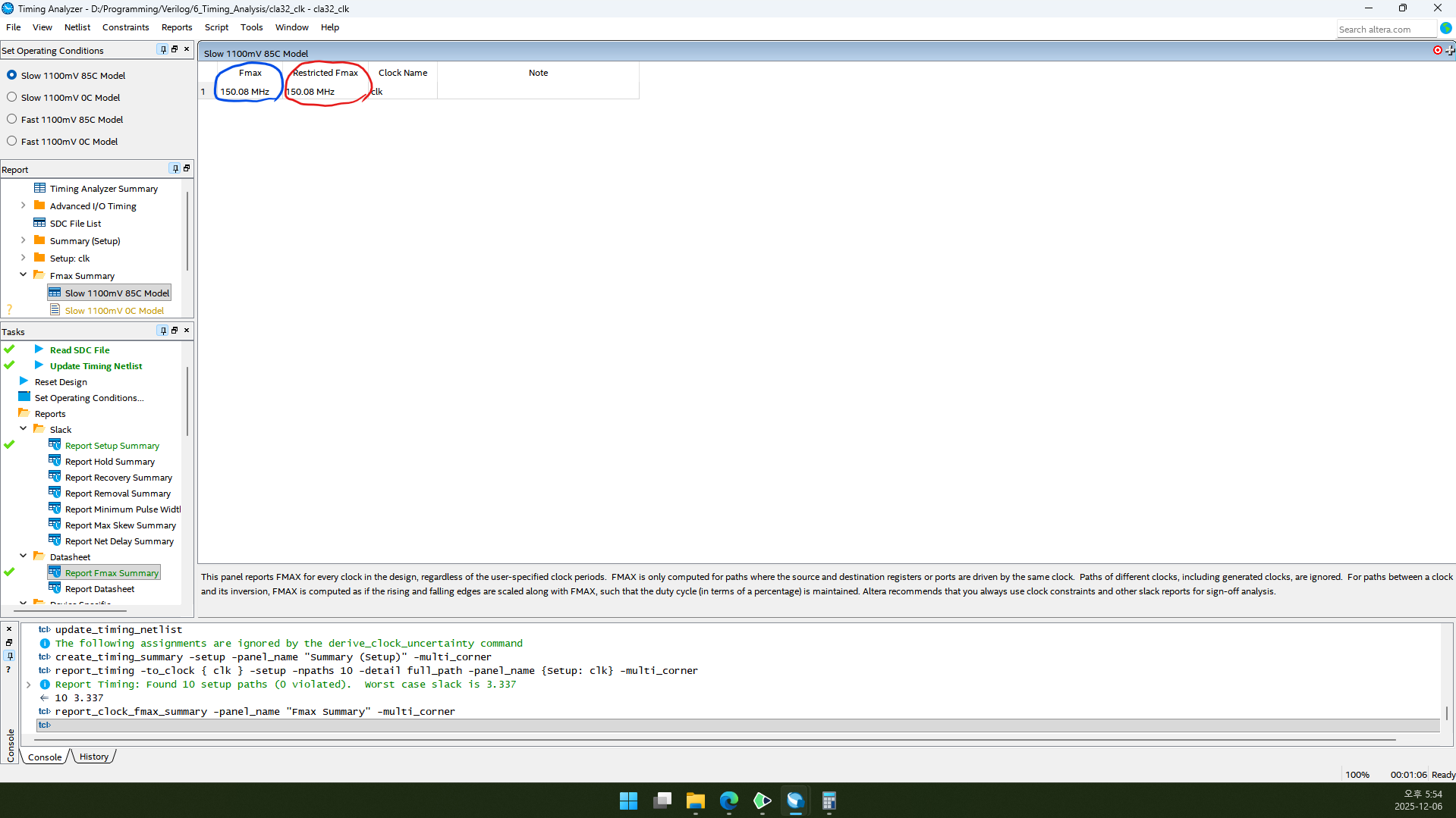
2.25. Fmax와 Restricted Fmax를 확인할 수 있습니다.
Fmax는 회로가 작동할 수 있는 최대 frequency입니다.
Restricted Fmax는 FGPA device limit을 고려한 최대 frequency로써, Fmax보다 클 수 있습니다.
일단 오늘 회로는 둘 다 150.08MHz가 나왔네요. 최대 frequency는 150.08MHz가 되겠습니다. 최소 주기는 150.08MHz의 역수가 되겠지요.
3. 글 마무리
제 글을 읽어 주셔서 감사합니다. 다음에 만나요!
4. 참고 자료
1) Intel Corporation. n. d. “fmax Definition”, Intel® Quartus® Prime Pro Edition Help version 22.1. (2025. 12. 06. 방문). https://www.intel.la/content/www/xl/es/programmable/quartushelp/22.1/index.htm#reference/glossary/def_fmax.htm